Artificial intelligence is revolutionizing every aspect of electronics manufacturing, and PCB design is no exception. Machine learning algorithms are now capable of optimizing PCB layouts, predicting signal integrity issues, and reducing design cycles from weeks to days.
The integration of AI into PCB design tools represents one of the most significant advances in electronic design automation (EDA) in decades. Companies adopting these technologies report dramatic improvements in design quality, reduced respins, and faster time-to-market.
The Evolution of AI in Electronics Design
AI applications in PCB design have evolved rapidly from simple rule-based checking to sophisticated machine learning systems capable of understanding complex design relationships and making intelligent decisions. This evolution has been driven by advances in AI algorithms, increased computing power, and the accumulation of vast design databases that can be used for training.
Early AI tools for PCB design focused on design rule checking (DRC), ensuring that layouts complied with manufacturing capabilities and design guidelines. While useful, these tools were limited to identifying violations of predefined rules. Modern AI systems go far beyond, learning from historical designs to optimize layouts in ways that human designers might not consider.
Key Applications of AI in PCB Design
Automated Component Placement
Component placement is one of the most critical and time-consuming aspects of PCB design. AI-powered placement algorithms consider dozens of interconnected factors simultaneously: signal integrity requirements, thermal management, manufacturing constraints, and mechanical specifications. Machine learning systems trained on thousands of successful designs can identify optimal placements that balance all these considerations.
These algorithms continuously learn from design outcomes, refining their understanding of what makes a successful placement. Designs that experienced field failures or manufacturing issues provide training data that helps the AI avoid similar problems in future designs.
Routing Optimization
AI routing engines go beyond simple pathfinding to optimize routes for signal integrity, crosstalk minimization, and impedance control. Traditional routing algorithms find valid paths but may not optimize for electrical performance. AI-enhanced routing considers the entire signal chain, minimizing reflections, controlling characteristic impedance, and reducing coupled noise between adjacent traces.
For high-speed designs, AI routing can be transformative. The system learns from electromagnetic simulations and field measurements, improving its ability to predict and avoid signal integrity issues before physical prototypes are built.
Design for Manufacturing Analysis
AI systems excel at predicting manufacturing challenges before designs reach production. By analyzing historical manufacturing data, these tools can identify features that might cause yields problems, such as thin traces that may break during handling, via structures that may fail under thermal stress, or component placements that create assembly difficulties.
Design for manufacturing (DFM) analysis powered by AI provides actionable recommendations with specific severity levels, allowing designers to prioritize their corrections effectively.
Reducing Development Time and Cost
The most immediate benefit companies experience when adopting AI-powered design tools is reduced development time. Design cycles that previously took six to eight weeks can often be completed in two to three weeks with AI assistance. This acceleration comes from multiple sources:
- Faster Iteration: AI tools enable rapid exploration of design alternatives, allowing engineers to evaluate more options in less time.
- Fewer Design Errors: Intelligent rule checking catches issues early, before they propagate through the design and require extensive rework.
- Automated Documentation: AI systems can automatically generate manufacturing documentation, test procedures, and regulatory compliance reports.
- Knowledge Transfer: AI captures design knowledge from experienced engineers, making it available to less experienced team members.
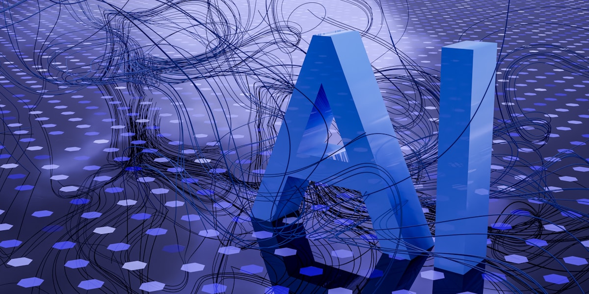
AI-powered design optimization algorithms
Beyond time savings, AI tools reduce costs by minimizing design respins. Each PCB respin can cost tens of thousands of dollars in engineering time, delayed product launches, and expedited manufacturing. AI's ability to catch issues before fabrication significantly reduces these costs.
Signal Integrity Improvement
As signal speeds continue to increase, maintaining signal integrity becomes increasingly challenging. AI tools are particularly valuable for high-speed designs where traditional design methods may miss subtle issues that cause reliability problems or electromagnetic interference.
Machine learning models can predict signal integrity issues based on layout features, component placement, and routing topology. By learning from thousands of designs that have been validated through simulation and physical testing, these models develop intuitions about which combinations of features are likely to cause problems.
AI-powered signal integrity analysis goes beyond identifying problems to suggesting specific remedies. When the system detects a potential crosstalk issue, it might recommend adjusting trace spacing, adding ground planes, or changing layer assignments—all with predictions of the expected improvement.
Design Space Exploration
Perhaps the most powerful capability of AI in PCB design is its ability to explore vast design spaces that would be impractical for human designers to consider. AI systems can generate and evaluate thousands of design variations, optimizing for multiple objectives simultaneously.
This capability is particularly valuable when optimizing for trade-offs between competing requirements. A design might need to balance size, cost, performance, and reliability. AI optimization algorithms can navigate this complex multi-dimensional space, identifying Pareto-optimal solutions that represent the best possible trade-offs.
Designers can interact with these systems, constraining certain parameters and guiding the optimization toward preferred solutions. The result is a collaborative process where human judgment and machine capability combine to produce superior outcomes.
Challenges and Considerations
While AI offers tremendous benefits for PCB design, successful implementation requires attention to several factors. Training data quality is critical—AI systems are only as good as the data they're trained on. Organizations need access to well-documented historical designs with known outcomes to train effective models.
Integration with existing design workflows is another consideration. AI tools work best when they integrate seamlessly with established EDA platforms rather than requiring completely new processes. Fortunately, most major EDA vendors now offer AI-enhanced versions of their tools.
Human oversight remains essential. AI systems make mistakes, and their recommendations should always be reviewed by experienced engineers. The most effective approach treats AI as a powerful assistant that augments human capabilities rather than replacing human judgment entirely.
The Future of AI in PCB Design
The trajectory of AI in PCB design points toward increasingly sophisticated capabilities. Generative AI—systems that can create designs from specifications rather than optimizing existing layouts—shows promise for automating routine design tasks. These systems could potentially generate complete PCB layouts from netlists and requirements documents, with human designers providing high-level guidance and review.

The future of AI-driven electronics design
Integration across the entire electronics development process is another frontier. AI systems that understand the complete product lifecycle—from concept through design, manufacturing, testing, and field operation—could optimize designs not just for individual metrics but for overall product success.
As AI capabilities continue to expand, the role of PCB designers will evolve. Routine tasks will increasingly be automated, freeing designers to focus on creative problem-solving, system-level optimization, and innovation. Engineers who learn to collaborate effectively with AI systems will be well-positioned for success in this evolving landscape.
Ready to Experience AI-Optimized PCB Manufacturing?
Partner with YS CIRCUIT for your next PCB project.
Contact Us