High-Density Interconnect (HDI) PCBs are fundamentally transforming how we design and manufacture electronic devices. As consumer demand for smaller, faster, and more powerful gadgets continues to accelerate, the electronics manufacturing industry has turned to HDI technology to meet these increasingly stringent requirements.
The global HDI PCB market is experiencing unprecedented growth, driven primarily by the proliferation of smartphones, wearable devices, and the expanding Internet of Things (IoT) ecosystem. Industry analysts project the HDI PCB market to exceed $20 billion by 2030, representing one of the fastest-growing segments in the printed circuit board industry.
Understanding HDI PCB Technology
HDI PCBs are defined by their higher wiring density per unit area compared to traditional circuit boards. This increased density is achieved through several advanced manufacturing techniques that allow for finer lines, smaller vias, and closer component spacing.
The key characteristics that distinguish HDI PCBs include:
- Microvias: HDI boards utilize microvias with diameters of 0.15mm or smaller, compared to traditional via sizes of 0.3mm and above. These microscopic drill holes allow for more efficient routing of signals between layers.
- Fine Line Widths: HDI technology enables line widths and spacings of 0.075mm (3 mil) or less, significantly finer than the 0.15mm typically achievable with standard PCB manufacturing.
- Layer Density: HDI boards can pack more functionality into fewer layers, reducing overall board thickness and material costs.
- Buried and Blind Vias: Unlike through-hole vias that traverse the entire board, blind vias connect an outer layer to an internal layer, while buried vias connect internal layers without reaching the surface. This technology maximizes routing flexibility.
Benefits of HDI PCB Implementation
The adoption of HDI technology offers manufacturers and product designers numerous advantages that extend beyond mere size reduction. Understanding these benefits helps explain why HDI has become the preferred choice for cutting-edge electronic products.

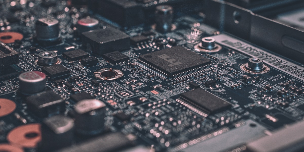
HDI PCB manufacturing requires precision equipment for microvia drilling
Size and Weight Reduction
One of the most immediate benefits of HDI PCBs is the significant reduction in board size and overall product weight. By enabling more circuits to be routed in a smaller footprint, HDI technology allows manufacturers to create slimmer, more compact devices. This characteristic has been particularly valuable in the smartphone industry, where device thickness continues to decrease while functionality increases.
A typical HDI smartphone motherboard might utilize 8-12 layers with microvia technology, compared to 14-16 layers required with conventional PCB technology to achieve the same functionality. This translates directly to reduced material costs, simplified assembly, and improved thermal performance.
Improved Electrical Performance
HDI PCBs deliver superior electrical performance due to shorter signal paths and reduced via stub lengths. The fine line geometries and controlled impedance characteristics of HDI boards result in lower signal attenuation, reduced electromagnetic interference (EMI), and improved signal integrity at high frequencies.
These electrical advantages make HDI PCBs particularly suitable for high-speed digital applications, including 5G communications equipment, high-performance computing systems, and advanced driver assistance systems (ADAS) in automobiles.
Enhanced Reliability
Despite their increased complexity, HDI PCBs can offer improved reliability compared to traditional multilayer boards. The reduced via stub lengths minimize signal reflections and impedance discontinuities that can lead to signal integrity issues. Additionally, the buried and blind via configurations reduce stress points that can crack during thermal cycling.
Applications Across Industries
The versatility of HDI PCB technology has led to widespread adoption across numerous industries, each leveraging specific advantages to meet unique requirements.
Consumer Electronics
The consumer electronics sector remains the largest consumer of HDI PCBs. Smartphones, tablets, smartwatches, and wireless earbuds all rely heavily on HDI technology to deliver compact form factors with maximum functionality. The latest smartphone designs routinely incorporate HDI boards with 12 or more layers, hundreds of components, and thousands of nets all packed into a footprint measuring just a few square centimeters.
Automotive Electronics
Modern vehicles have become sophisticated computers on wheels, with advanced infotainment systems, autonomous driving features, and extensive sensor networks. These applications demand PCBs that can operate reliably across wide temperature ranges while meeting strict size and weight constraints. HDI PCBs have become essential in automotive applications, particularly for engine control units (ECUs), advanced driver assistance systems, and in-vehicle networking equipment.
Medical Devices
Medical equipment manufacturers have embraced HDI technology for portable imaging devices, patient monitoring systems, and implantable medical devices. The reduced size of HDI PCBs enables the development of less invasive surgical tools and more comfortable wearable health monitors. Furthermore, the improved reliability of HDI boards aligns with the demanding quality requirements of medical applications.
Manufacturing Considerations and Challenges
While HDI PCB technology offers compelling advantages, it also presents significant manufacturing challenges that require specialized equipment, expertise, and quality control processes.

Advanced manufacturing equipment for HDI PCB production
Advanced Manufacturing Equipment
Producing HDI PCBs requires precision manufacturing equipment capable of achieving the extremely tight tolerances demanded by fine line and space geometries. This includes advanced photolithography systems, precision drilling equipment for microvia formation, and sophisticated layer-to-layer registration systems.
YS CIRCUIT has invested heavily in state-of-the-art manufacturing capabilities to support HDI PCB production. Our facilities feature laser drilling systems capable of creating microvias with diameters as small as 0.1mm, achieving registration accuracies of ±0.025mm across multiple layers.
Material Selection
The choice of substrate materials becomes critical in HDI PCB manufacturing. High-frequency applications may require specialized dielectric materials with controlled electrical properties, while high-reliability applications demand materials with excellent thermal stability and mechanical strength.
Common HDI substrate materials include standard FR-4 grades for cost-sensitive applications, high-Tg FR-4 for enhanced thermal performance, and advanced materials such as polyimide and low-loss laminates for demanding high-frequency applications.
Quality Assurance
Testing and inspection of HDI PCBs requires specialized approaches due to the microscopic features involved. Automated optical inspection (AOI) systems must be calibrated for the finer geometries, while electrical testing must account for the increased net densities and more complex routing patterns.
YS CIRCUIT maintains rigorous quality control procedures throughout the HDI manufacturing process, including statistical process control, first-pass yield monitoring, and comprehensive electrical testing using flying probe and fixture-based techniques.
Future Trends in HDI Technology
The evolution of HDI PCB technology continues at a rapid pace, driven by emerging applications and advancing manufacturing capabilities. Several trends are shaping the future of this critical technology.
Ultra-high-density interconnect (UHDI) technologies are emerging, targeting even finer line geometries and smaller via sizes. These advanced processes aim to achieve line widths below 0.05mm (2 mil) and via diameters under 0.1mm, enabling further miniaturization of electronic devices.
Embedded component technology is gaining traction as a complementary approach to HDI. By embedding passive components and even active ICs within the PCB substrate, manufacturers can achieve even greater density improvements while reducing assembly steps and potential failure points.
The integration of object-like 3D structures is another frontier being explored by PCB designers and manufacturers. Rather than purely planar designs, 3D-MID (Three-Dimensional Molded Interconnect Devices) technology enables the creation of mechanical and electrical features in three dimensions, opening new possibilities for compact, multifunctional devices.
Choosing the Right HDI PCB Partner
Successful implementation of HDI technology requires careful selection of a manufacturing partner with demonstrated expertise, appropriate capabilities, and a commitment to quality. When evaluating potential HDI PCB suppliers, consider the following factors:
- Technical Capabilities: Verify that the manufacturer can produce boards meeting your specific requirements for line/space, via size, layer count, and material selection.
- Quality Certifications: Look for relevant certifications such as ISO 9001, AS9100 (for aerospace applications), and IATF 16949 (for automotive). These certifications indicate a mature quality management system.
- Experience: Consider the manufacturer's track record with similar projects and their ability to provide design for manufacturing (DFM) feedback.
- Communication: Effective collaboration between designer and manufacturer is crucial for HDI projects. Choose a partner who provides responsive technical support and clear communication throughout the process.
At YS CIRCUIT, we combine decades of HDI PCB manufacturing experience with cutting-edge facilities to deliver high-quality boards that meet the most demanding specifications. Our engineering team works closely with customers from design through production to ensure optimal outcomes.
Conclusion
HDI PCB technology has evolved from a specialized niche to an essential enabler of modern electronics. As devices continue to demand greater functionality in smaller packages, HDI will remain at the forefront of PCB innovation. Understanding the capabilities, benefits, and challenges of HDI technology empowers designers and engineers to make informed decisions about their PCB requirements.
Whether you're developing the next generation of smartphones, automotive electronics, or medical devices, HDI PCB technology offers the density and performance characteristics necessary to bring your vision to life. Contact YS CIRCUIT today to discuss how our HDI manufacturing capabilities can support your next project.
Ready to Start Your HDI PCB Project?
Get a quote for your HDI PCB requirements within 24 hours.
Contact Us