
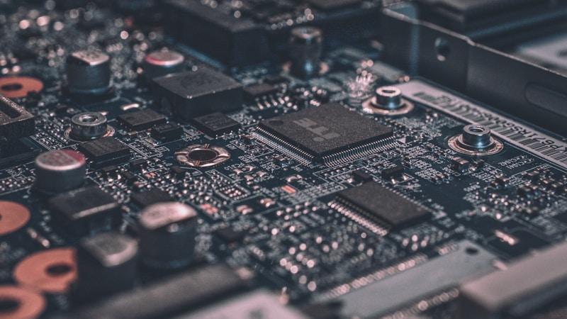
The intersection of artificial intelligence and electronics design represents one of the most exciting developments in the PCB industry. Generative AI systems can now create optimized circuit board layouts from high-level specifications, exploring design alternatives that human engineers might never consider. This technology is fundamentally changing how we approach PCB development.
How Generative AI Works in PCB Design
Unlike traditional electronic design automation (EDA) tools that optimize step-by-step, generative AI approaches PCB design as an optimization problem. Given a set of constraints—component locations, signal requirements, manufacturing rules, and performance specifications—these systems can generate multiple viable layouts simultaneously.
The AI learns from millions of existing designs, understanding the relationships between component placement, trace routing, signal integrity, and manufacturing yield. When generating new designs, it applies this learned knowledge to create layouts that balance performance, manufacturability, and cost.
From Specifications to Layouts
The generative design process begins with engineers inputting their requirements: component list, signal groupings, power requirements, thermal constraints, and physical specifications. The AI then generates multiple design alternatives, each representing a different approach to meeting those requirements.
Engineers can evaluate these alternatives based on various metrics—signal integrity, power delivery, thermal performance, EMI characteristics, and manufacturing cost. This approach shifts the engineer's role from creating designs to curating and refining AI-generated options.
Benefits of Generative PCB Design
- Explore 50+ design alternatives in minutes
- Optimize for multiple objectives simultaneously
- Automatic DFM rule compliance
- Reduced engineering hours per project
Optimizing for Multiple Objectives
Real-world PCB design involves balancing competing objectives. A design that optimizes for signal integrity might be more expensive to manufacture. A layout that minimizes board size might create thermal challenges. Generative AI excels at multi-objective optimization, finding the Pareto-optimal solutions that represent the best possible trade-offs between competing requirements.
This capability is particularly valuable for complex boards with mixed-signal content, high-speed interfaces, or tight form factors. Engineers can quickly identify which designs offer the best balance of performance, cost, and reliability for their specific application.
The Human-AI Collaboration
Despite its capabilities, generative AI doesn't replace human expertise—it amplifies it. Engineers remain essential for setting design intent, validating AI-generated solutions, and applying domain knowledge that AI may not fully capture. The most successful implementations treat generative AI as a powerful tool in the engineer's toolkit rather than a replacement for human judgment.
As these tools mature, we expect to see them become standard fixtures in PCB design workflows, enabling smaller teams to tackle increasingly complex designs while maintaining quality and accelerating delivery schedules.


